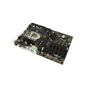
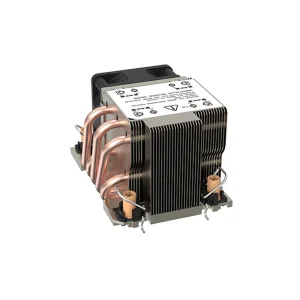
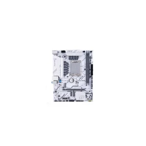
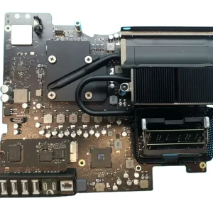
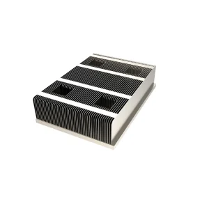
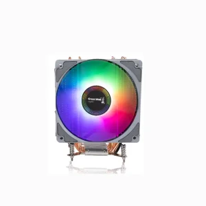
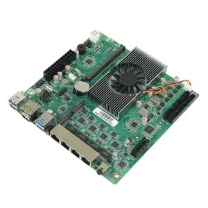
Browse our integrated collection of high-performance server heatsinks, heavy copper substrate applications, and desktop hardware essentials optimized for intense heat dissipation.
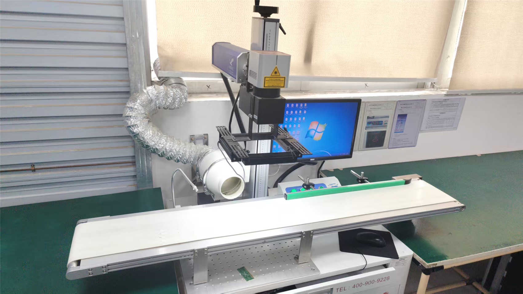
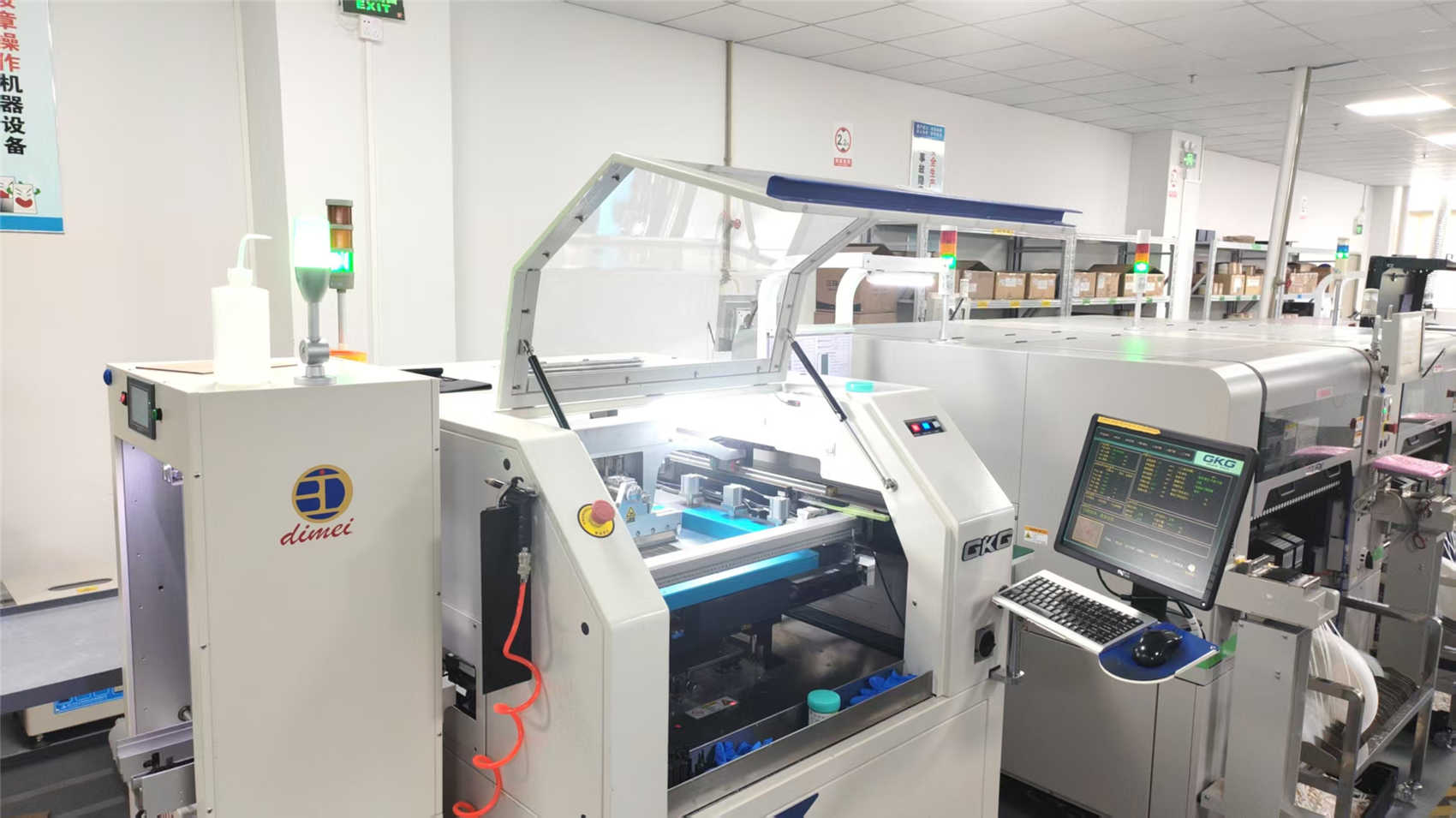
In the evolving landscape of power electronics, the demand for Thick Copper Circuit Boards (conventionally defined as boards featuring 3 oz/ft² to over 20 oz/ft² of copper thickness) has escalated. These specialized substrates are designed to conduct significantly higher current loads while operating as integrated thermal heat sinks, distributing heat away from localized components directly to the exterior. As semiconductors shrink and current densities rise in systems like AI computing chips, 5G base stations, and electric vehicle (EV) drivetrains, the circuit board is no longer just a passive connector; it is a critical thermodynamic and electromagnetic management layer.
Thick copper boards are distinguished from standard PCBs through their unique manufacturing parameters and operational capacities. These characteristics directly affect raw signal propagation, power distribution integrity, and the physical lifespan of finished assemblies:
The roadmap for heavy copper technology points directly towards integration with High-Density Interconnect (HDI) structures and embedded component technologies. Over the next decade, developers and global manufacturers must address technical barriers associated with etching accuracy, solder mask application over elevated copper profiles, and hybrid lamination architectures.
Combining heavy copper layers (up to 12 oz) for power delivery with standard 1 oz signal layers on a single substrate to reduce overall board thickness and optimize signal integrity in multi-layer stackups.
Integrating ceramic-based copper modules inside traditional organic FR4 layers to support high-voltage components in renewable energy converters and EV charging stations.
Implementing advanced chemical etching agents and dry-film photoresist formulations to maintain clean vertical side-walls on trace paths exceeding 15 oz copper thickness, preventing trace necking.
Transitioning toward 3D printed trace architectures where copper sheets over 30 oz are selectively integrated with polymer frames, shaping the next generation of high-current industrial switchgear.
Modern electrical assemblies require holistic thermodynamic designs. Standard layouts fail under severe stresses; this is where heavy copper substrates step in to provide robust systems across multiple modern vertical fields.
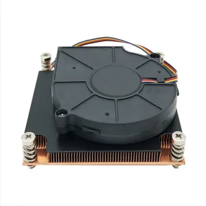
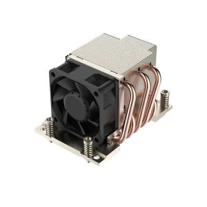
Deploying heavy copper layers ensures low-resistance power distribution paths directly to high-draw CPU and GPU arrays, working in tandem with server coolers like the 350W AMD SP6 Heatsink.
Heavy copper tracks enable rapid charging compatibility, battery monitoring systems, power inverters, and planar transformers, handling massive continuous currents while resisting road vibration.
Low resistance is key to eliminating audio signal loss. In high-fidelity audio structures like the FR4 Audio Decoder Assembly, heavy copper paths maximize SNR (Signal to Noise Ratio).
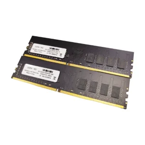
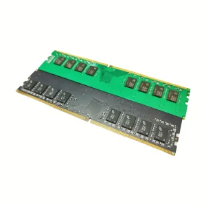
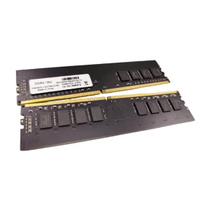
To understand the implementation of complex circuits, one must look at leaders in high-performance electronics manufacturing. CoreByte Storage Technology Co., Ltd. stands as a premier manufacturer specializing in DDR5 memory, DRAM solutions, and high-performance system assemblies designed for global OEM, enterprise, and data center applications.
Company Established
Annual Export Revenue
Quality Inspectors
R&D Engineers
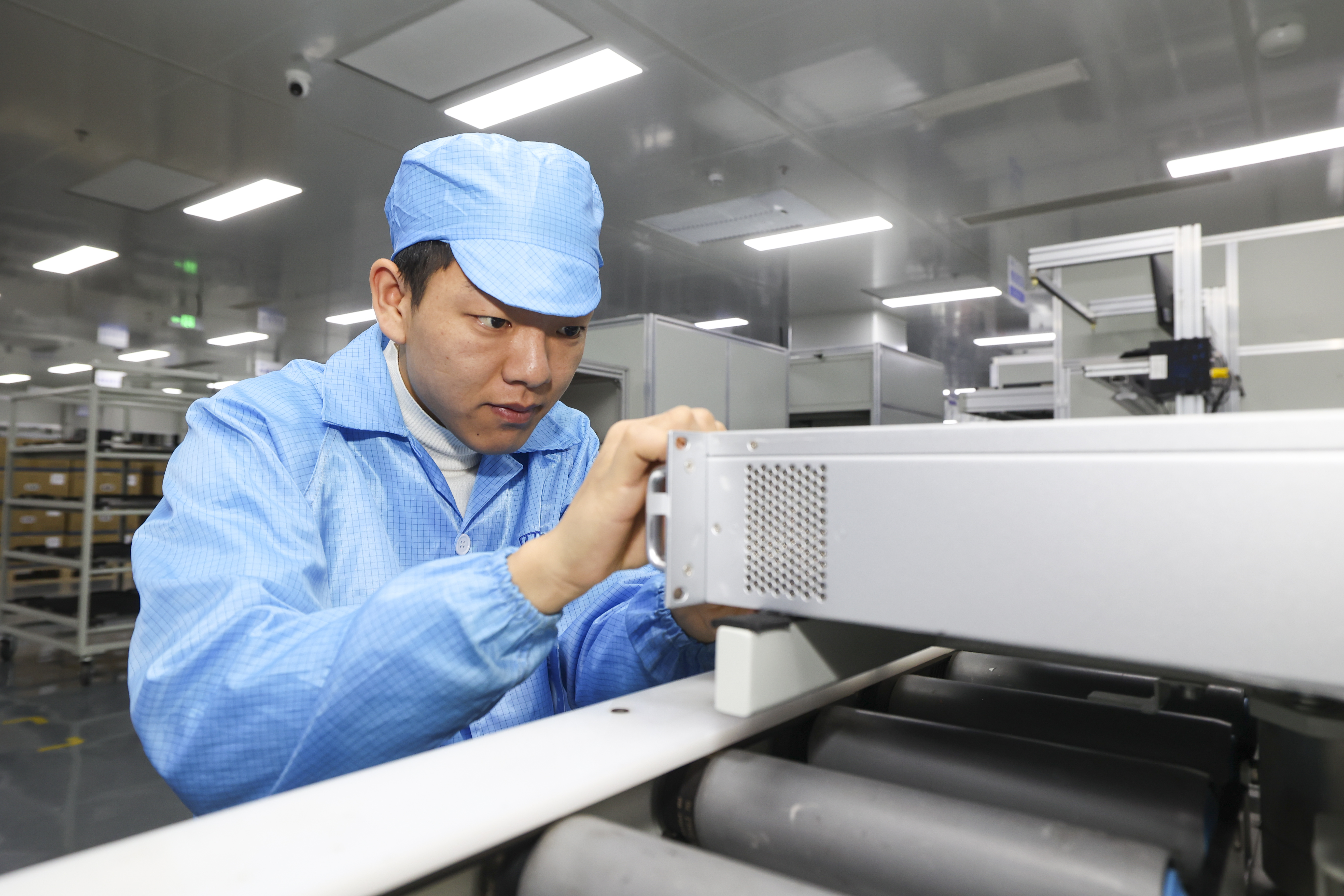
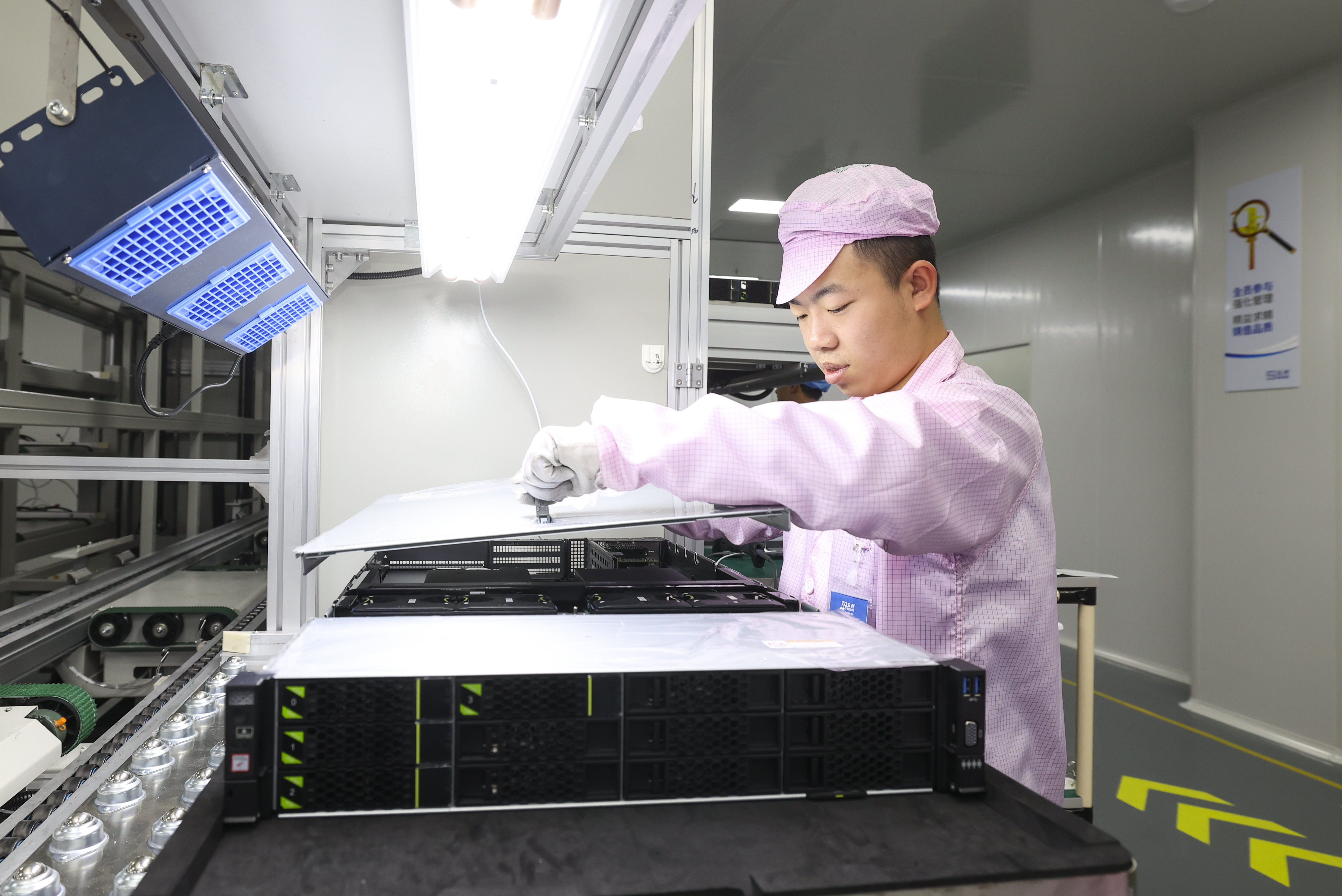
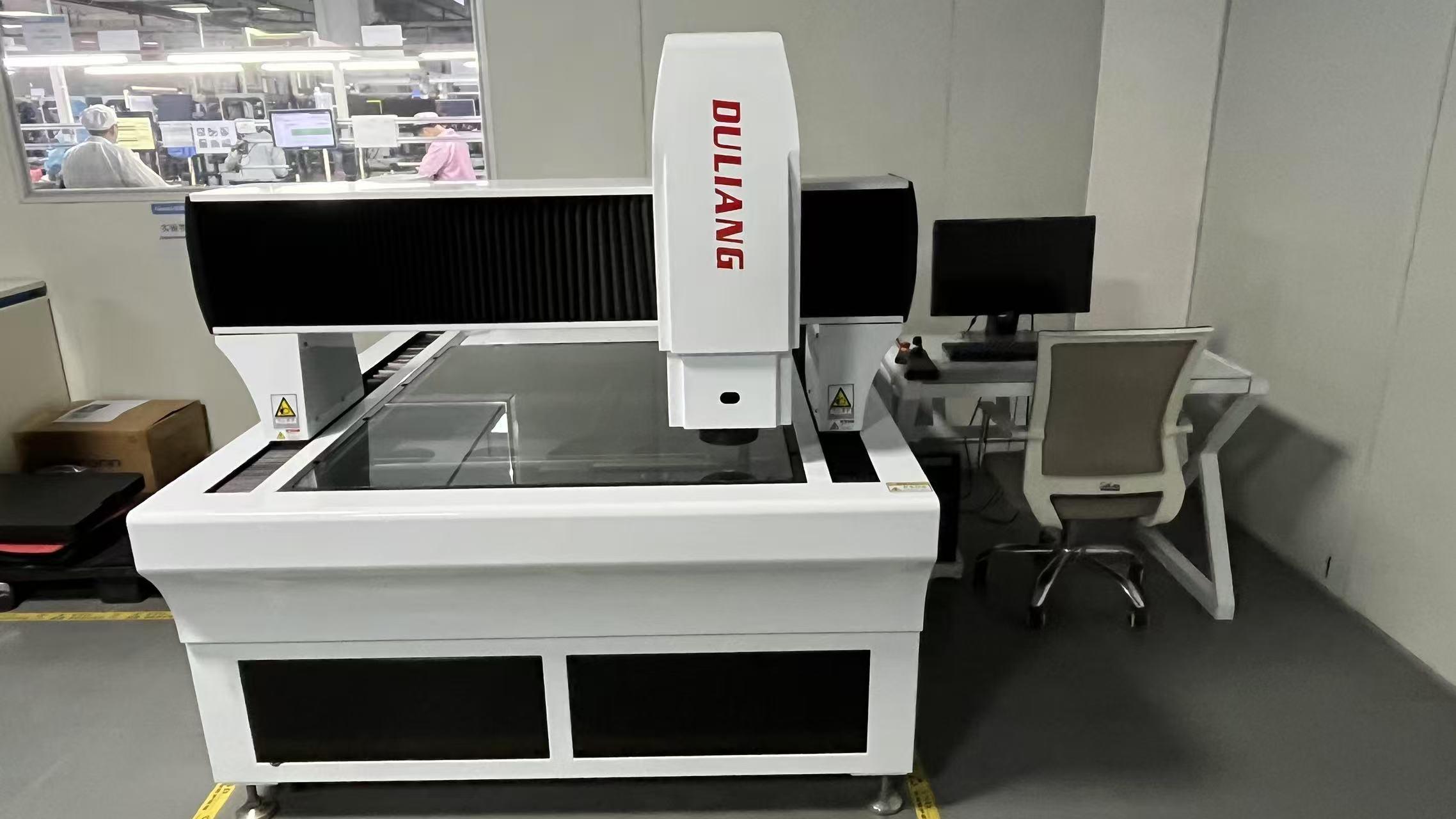
Established in 2016, CoreByte has developed strong capabilities in R&D, production, and international trade, focusing on stable, high-speed, and energy-efficient memory products. The company operates a modern manufacturing facility with a total building area of approximately 320㎡, equipped with advanced production and testing equipment to ensure strict quality control standards. Quality assurance is a core priority at CoreByte. The company implements ISO9001-based quality management systems, combined with automated optical inspection (AOI) and high-temperature aging tests to ensure product stability and compatibility.
CoreByte maintains a strong trade-oriented business background, serving key markets including North America, Europe, Southeast Asia, and the Middle East. The company has established a reliable global supply chain network with more than 1,200 supply chain partners, supporting stable production and fast delivery. CoreByte offers advanced customization services, including PCB design optimization, frequency tuning, thermal solution adjustment, and branding customization.
Modern sourcing requires manufacturing hubs with reliable raw materials, sophisticated equipment, and fast turnaround. China's electronics ecosystem offers key structural benefits for global buyers sourcing heavy copper PCBs and high-capacity memory solutions:
Vertical Continuous Plating (VCP) lines ensure copper thickness is deposited uniformly inside high-aspect vias, avoiding weak points in current conduction paths.
Laser Direct Imaging (LDI) tools permit tight trace alignment on top of rugged base substrates, guaranteeing signal alignment in hybrid multi-layer stackups.
Immediate access to globally recognized copper foils and high-TG raw materials (such as Shengyi, Rogers, and KB laminates) secures optimal pricing and fast production lead times.
Integrated MES systems track every phase of production, providing automated material tracking, vacuum lamination logging, and 100% AOI inspection reports.
When selecting a top supplier for thick copper circuit boards, engineering procurement teams must look past basic cost-per-square-inch rates. The following technical criteria determine reliability and yield rate of complex boards:
Discover our range of enterprise memory options, motherboards, and server fans engineered to run smoothly inside demanding heavy-duty power layouts.