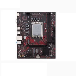
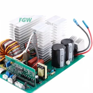
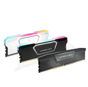
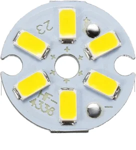
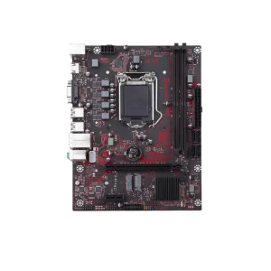
Engineered to support extreme bandwidth processing, high-density computing, and low-latency packet switching networks.
In the era of hyper-scale cloud operations, artificial intelligence (AI) scaling, and automated edge intelligence, the network infrastructure serves as the fundamental vascular system of enterprise operations. At CoreByte, we are witnessing a tectonic shift in network hardware architecture. Traditional proprietary, closed-box hardware systems are rapidly giving way to open, agile, and software-defined architectures. Modern enterprise operations demand network switches that are not just passive packet-forwarders, but active data-flow processors optimized for low latency, energy efficiency, and deterministic performance.
The growth of generative AI workloads and massive machine-to-machine communication protocols has accelerated the deployment of high-density switching engines. From multi-gigabit access points to 100G/400G and emerging 800G fabric layers in data centers, network switches now require advanced hardware virtualization, strict Time-Sensitive Networking (TSN) capabilities, and next-generation Power-over-Ethernet (PoE++ up to 90W) to power advanced automation, high-definition security arrays, and IoT gateways.
For enterprise network architects, systems integrators, and industrial purchasing managers, selecting a reliable network switch partner goes far beyond basic component datasheets. The modern supply chain requires strategic alignment across multiple operational vectors.
Zero-loss packet forwarding is mandatory. Hardware must endure rigorous signal attenuation, impedance matching, and electromagnetic interference (EMI) shielding to ensure clean packet transfers across ultra-long fiber and copper topologies.
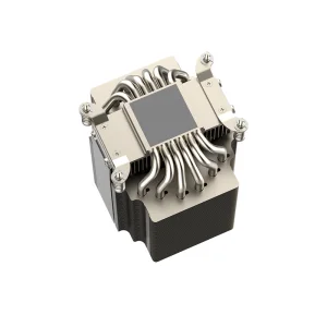
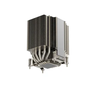
Operating temperatures in modern data centers and industrial plants can fluctuate wildly. Procured hardware must utilize advanced cooling architecture—such as custom liquid-cooling blocks, copper-jacketed passive heat sinks, and thermal dissipation layers—to maintain structural stability.
Enterprise networks are prime targets for physical and logical intrusion. Hardware-level security, incorporating trusted platform modules (TPM), tamper-detection circuitry, and cryptographically verified firmware signatures, is critical at the factory layout stage.
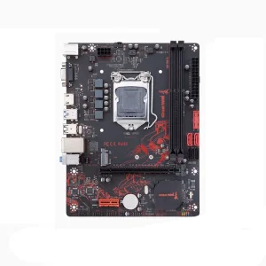
CoreByte Storage Technology Co., Ltd. operates at the intersection of robust supply chain orchestration and high-precision component manufacturing. Established in 2016, we have built a manufacturing and R&D ecosystem engineered to address global hardware challenges. Moving past simple circuit board assembly, our operations represent true Industry 4.0 integration: high-mix, low-volume flexibility coupled with massive production scaling, deep components traceability, and end-to-end quality validation.
With over 9 years of industry experience in high-performance memory, advanced semiconductor solutions, and multichip layout designs, CoreByte leverages a solid supply chain web of more than 1,200 verified partners. This ecosystem guarantees stable, uninterrupted procurement of high-speed packet processors, high-frequency FR4 laminates, passive components, and advanced thermal interfaces. Our manufacturing capability bridges high-frequency printed circuit boards, advanced DDR4/DDR5 system cache optimization, and cooling technologies to deliver highly resilient networking switches.
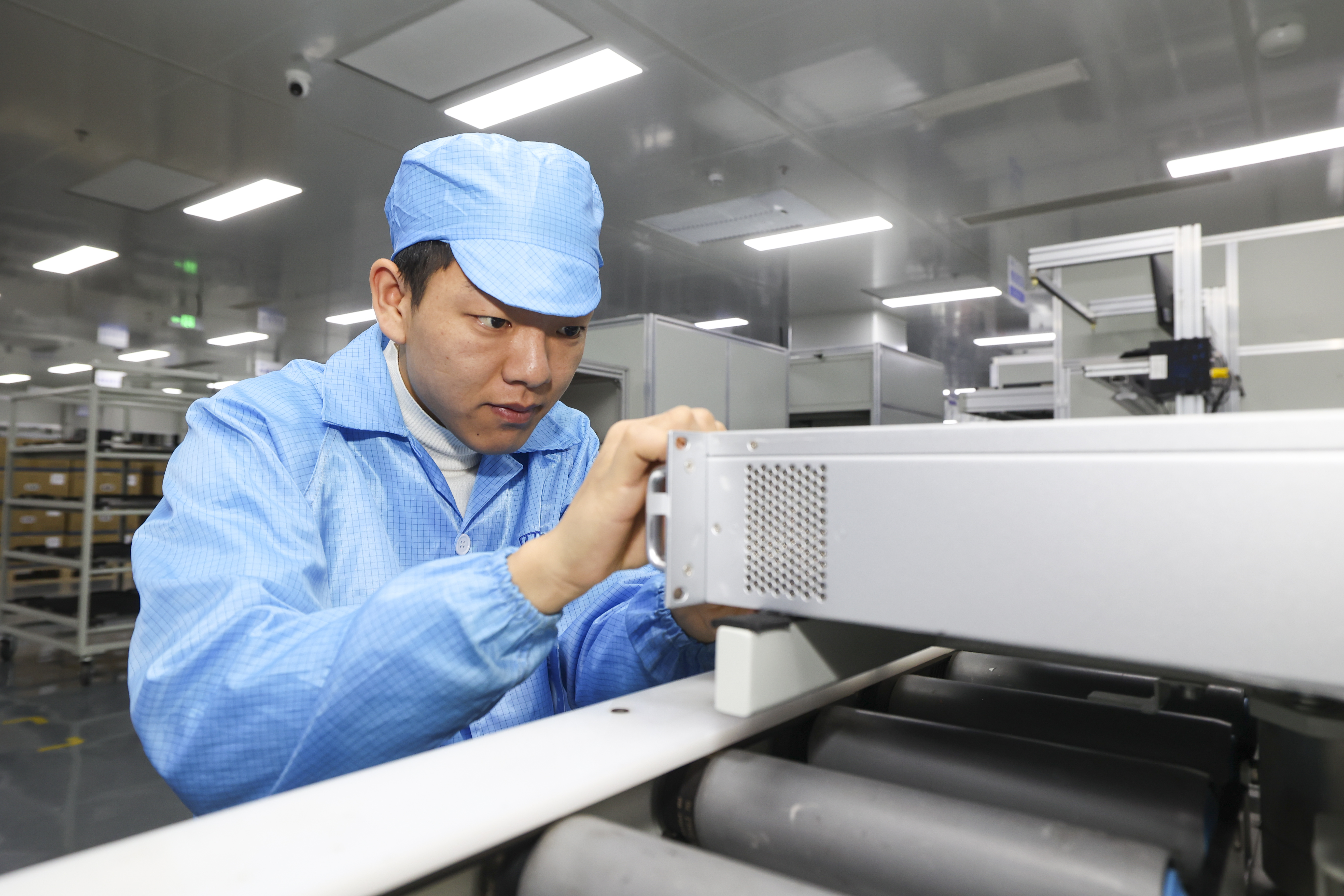
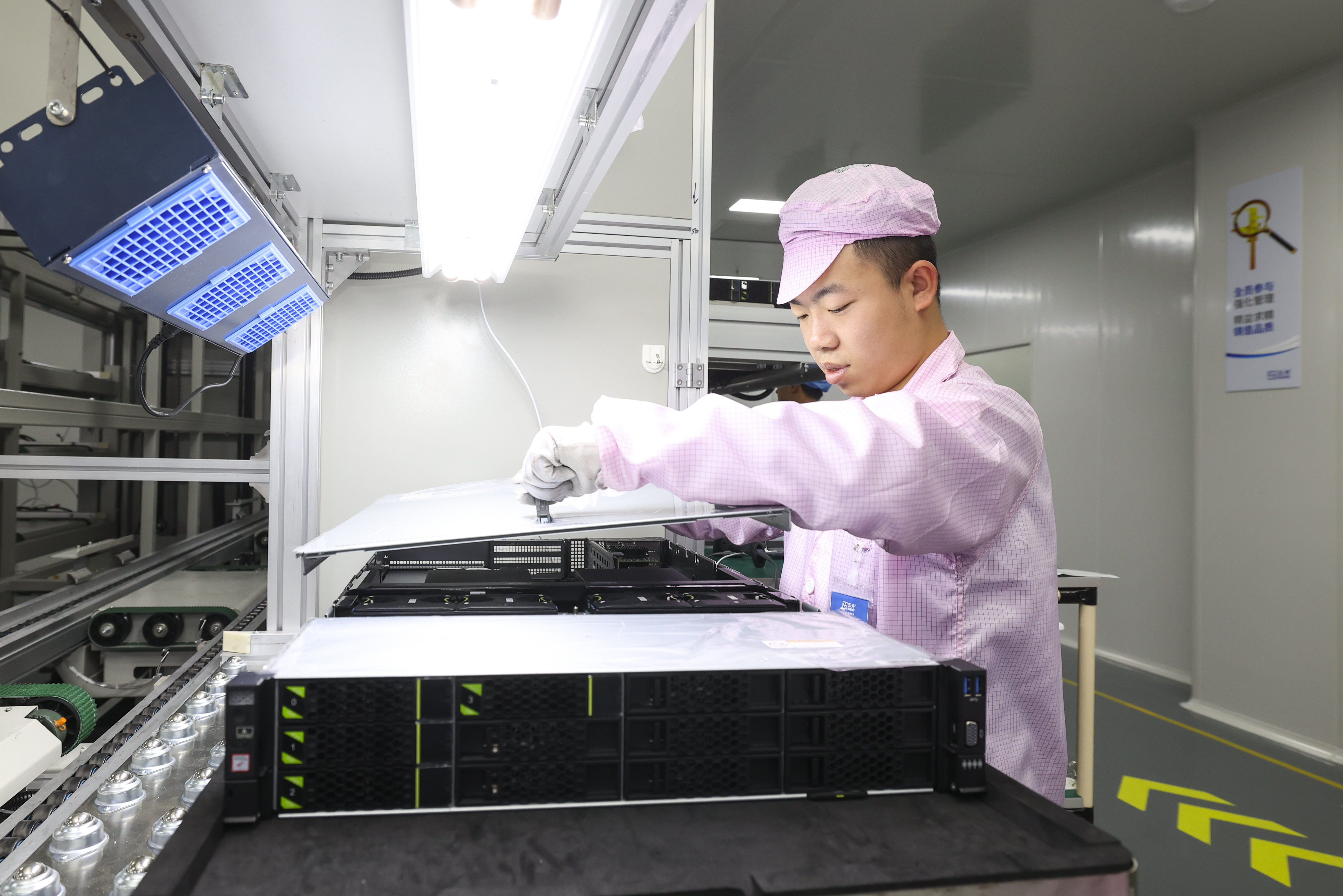
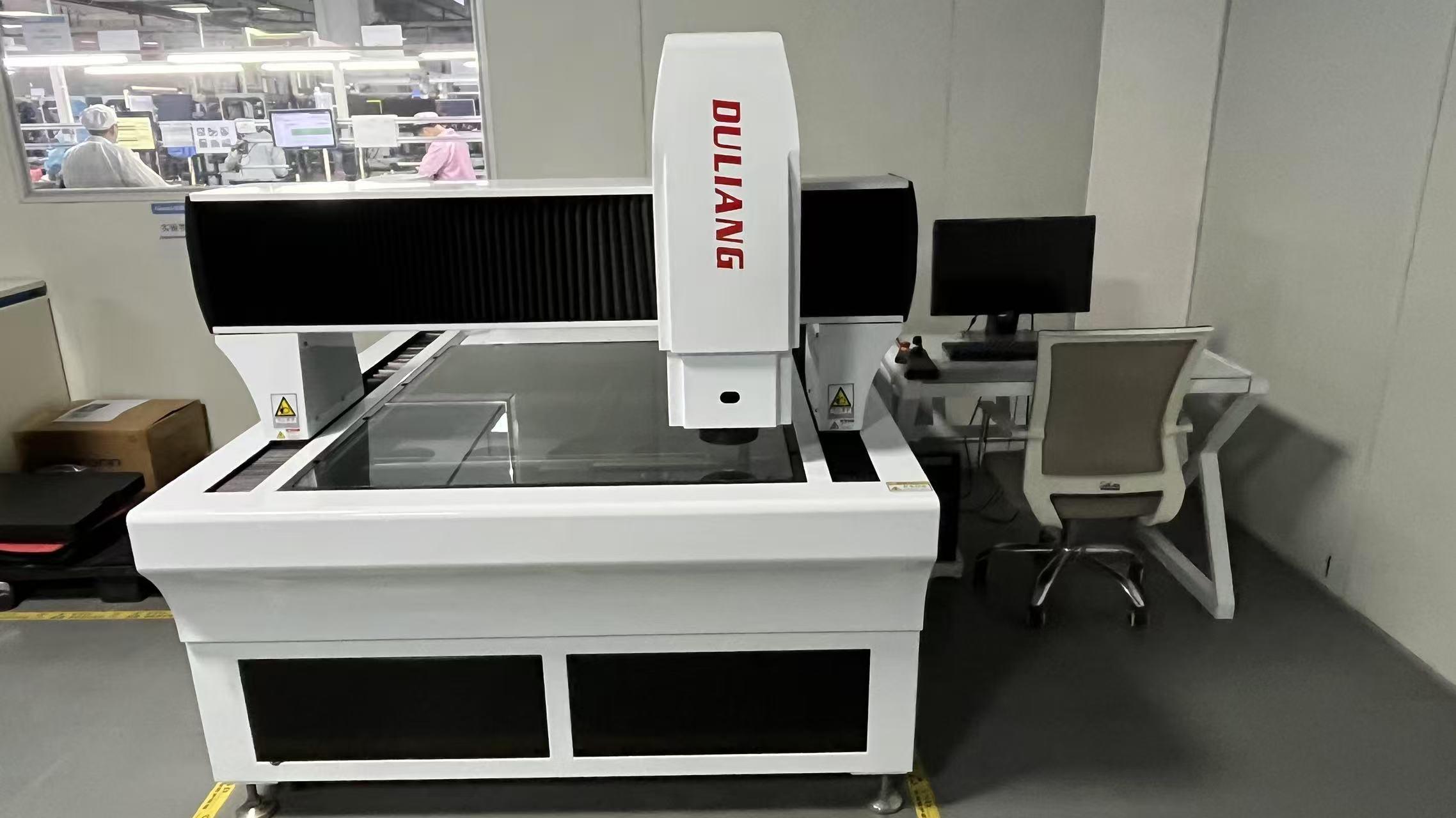
Every network switch, PCBA prototype, and memory module we produce must satisfy rigid performance mandates before deployment. Quality assurance at CoreByte is governed by an ISO9001-certified Quality Management System, executed by a highly specialized team of 45 dedicated quality inspectors.
Our assembly lines integrate Automated Optical Inspection (AOI) technology that visually scans 100% of PCBA layouts. By inspecting component placement accuracy, solder bridge formations, and microscopic solder fillet angles, we eliminate structural and electrical defects before systems reach the packaging stage.
Hardware components undergo extreme environmental stress screening (ESS). The fully populated boards are subjected to continuous high-temperature aging chambers under maximum processing loads. This process isolates early-life semiconductor failures, ensuring long-term hardware reliability under harsh operational parameters.
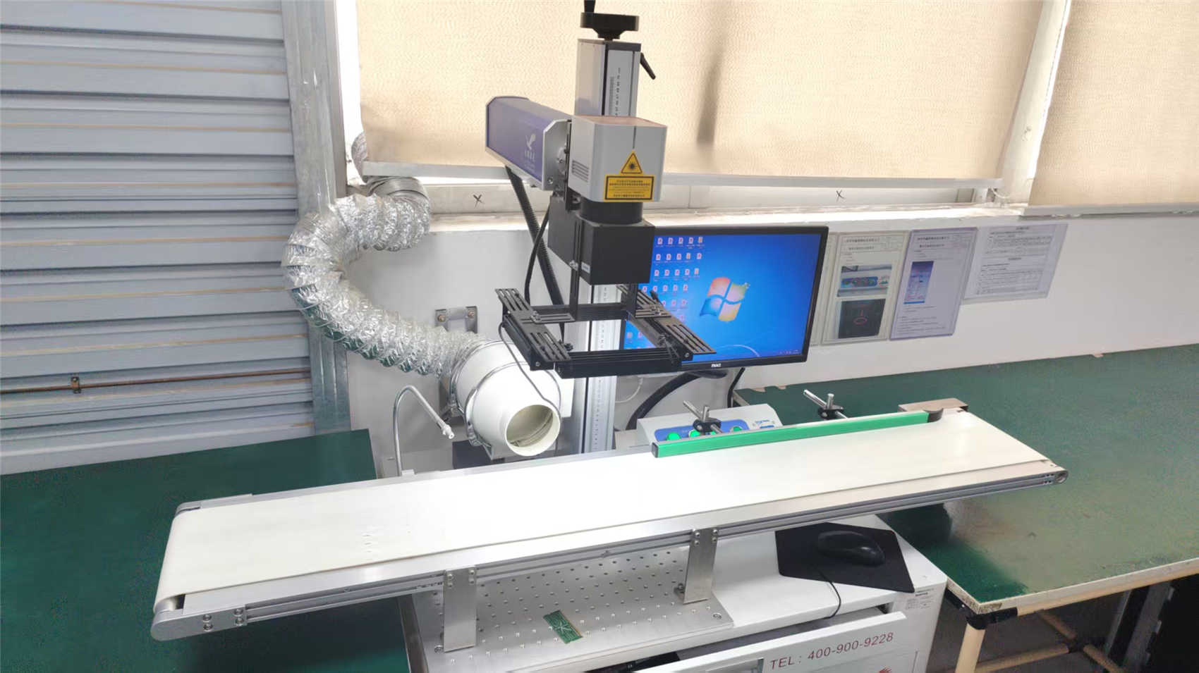
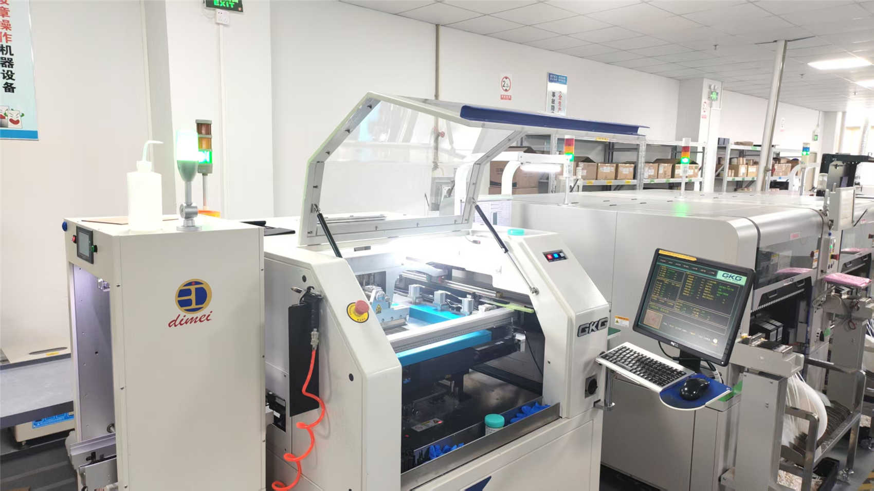
Modern networks require customized layouts based on physical environments, protocol loads, and bandwidth footprints. Our OEM/ODM capabilities adapt to several distinct infrastructure demands.
In leaf-spine architectures, high port density, low latency, and packet buffer efficiency are critical. Our switches incorporate enterprise-grade DDR5 buffering to prevent bottleneck congestion during heavy east-west data flow cycles.
Ruggedized environments present dust, vibration, and thermal challenges. We build fanless switches with wide temperature tolerance (-40°C to +85°C), heavy-gauge aluminum heat sinks, and surge protection interfaces.
Deploying IP cameras, outdoor access points, and dynamic sensory units requires high-wattage power delivery. Our switches support PoE+ and PoE++ (IEEE 802.3bt) to power distant edge devices over standard Ethernet lines.
Find technical insights into CoreByte's capabilities, design parameters, quality controls, and customized manufacturing services.
We provide complete end-to-end design and manufacturing options. This includes high-frequency PCB stack-ups, custom port physical arrangements (RJ45, SFP+, SFP28, QSFP28), specialized passive heat sinks or active fan layout cooling solutions, customized metal enclosure fabrication, branding, and pre-loading of customized boot loaders or open-source Network Operating Systems (such as SONiC or ONIE-based OS).
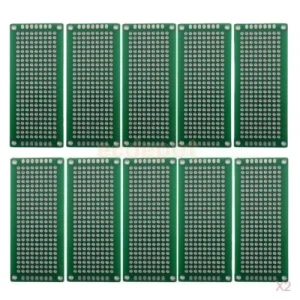
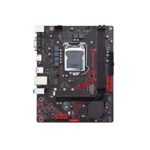
Our engineering division utilizes advanced simulation software to evaluate impedance matching, trace attenuation, and crosstalk before manufacturing. We use premium FR4 base boards and multilayer stack-ups with dedicated ground plane isolation to guarantee clean signal paths for high-speed differential signal pairs, ensuring reliable packet forwarding under maximum throughput conditions.
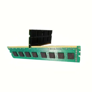
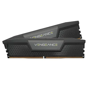
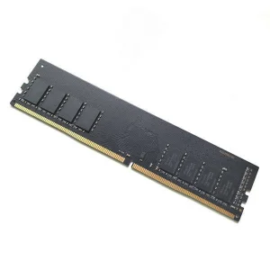
Yes. Given our extensive history as a DDR5 and DRAM memory module manufacturer, we are uniquely positioned to optimize the memory subsystem of our network switches. We integrate and tune high-speed, ECC-supported DRAM caching buffers directly onto the mainboard to assist the packet processing ASIC during intense traffic surges, eliminating packet loss during periods of congestion.
Our 45-inspector quality control team executes a rigorous multi-stage quality protocol. Every unit undergoes automated optical inspection (AOI) after SMT assembly, followed by high-frequency X-ray scans of BGA IC packages. Assembled switches then undergo high-temperature aging cycles under maximum workloads inside specialized testing chambers to isolate and replace any unstable components before final shipping.
We support the separation of software and hardware. Our OEM network switches can be configured with ONIE (Open Network Install Environment) bootloaders, enabling network administrators and system integrators to easily deploy custom Linux-based operating systems, Open Network Linux (ONL), or Microsoft SONiC distributions across global infrastructure deployments.
For standard customization, custom PCB prototypes are completed and tested within 3 to 4 weeks. Following prototype approval and environmental testing, our manufacturing lines can scale production rapidly. Mass production lead times vary from 4 to 6 weeks, depending on component availability and overall order volume, supported by our robust network of 1,200+ raw materials supply chain partners.
Industrial-grade control blocks, RAM modules, and layout components engineered for high uptime enterprise deployments.
 CoreByte