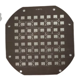
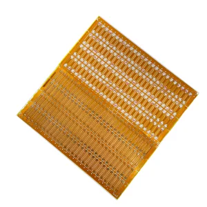
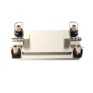
In the rapidly evolving landscape of electronics manufacturing, the Surface Mount Technology (SMT) process remains the bedrock of PCB assembly. At the heart of this process lies the Laser Cutting Stencil. As a leading OEM/ODM manufacturer, we understand that a stencil is not merely a piece of metal; it is the precision tool that dictates the yield, reliability, and thermal integrity of every circuit board produced. Whether for high-end server processors or consumer-grade gaming motherboards, the quality of solder paste deposition depends entirely on the stencil’s aperture geometry and material integrity.
At CoreByte, we have evolved our manufacturing philosophy to bridge the gap between memory/PCB production and the stencil tools required to assemble them. Our technical roadmap emphasizes Information Gain: we don't just sell products; we share the deep expertise required to achieve zero-defect SMT assembly.
Our capabilities include:
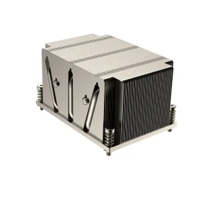
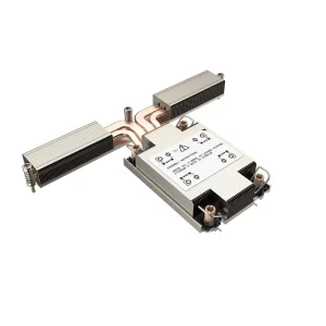
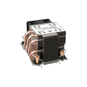
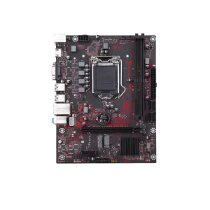
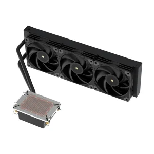
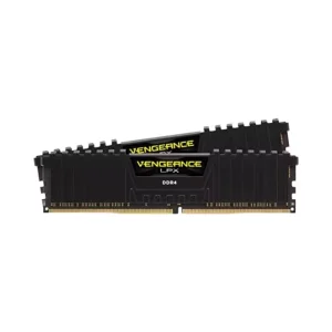
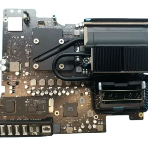
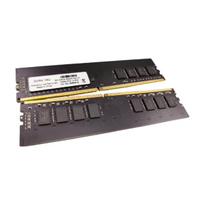
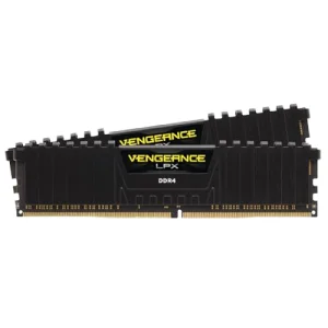
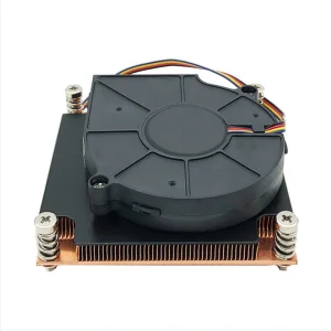
Global enterprises are shifting toward localized, "near-shore" supply chain models to mitigate geopolitical risks. Our role as an OEM/ODM provider is to act as an extension of your R&D team. We support procurement managers by offering integrated solutions—combining RAM, high-performance heat sinks (LGA4677, etc.), and the stencil tools needed to assemble them into finished products. This unified approach reduces vendor complexity and optimizes logistics costs.
The manufacturing landscape is moving toward Industry 4.0. We are currently investing in AI-driven aperture design software that predicts solder paste volume based on component density and thermal profiles. This proactive design philosophy ensures that by the time you reach mass production, the stencil design has already accounted for potential voiding issues, significantly increasing first-pass yield rates.
With 9 years of experience in the semiconductor and hardware sector, CoreByte Storage Technology Co., Ltd. has established a rigorous framework. Our manufacturing facility, while modern and compact, is packed with automated optical inspection (AOI) technology. Every stencil and every PCB module we ship undergoes stringent high-temperature aging tests and compatibility verifications.
Why Industry Leaders Choose Us:
In today's regulatory environment, compliance is non-negotiable. Our manufacturing processes fully comply with RoHS and REACH standards. We provide comprehensive documentation support for our clients in North America, Europe, and Southeast Asia, ensuring that your final products pass regulatory hurdles with ease. Our local support teams understand the time-zone challenges and are dedicated to providing responsive, real-time communication for urgent design changes or supply chain pivots.
Q: Why is stencil thickness so critical for my assembly?
A: Stencil thickness directly dictates the solder volume. Too thick, and you risk bridging (short circuits); too thin, and you face "open" joints. We calculate the aperture-to-thickness ratio (aspect ratio) to ensure optimal paste release.
Q: Can CoreByte handle both the PCB assembly materials and the stencil design?
A: Yes. We are uniquely positioned to offer an integrated service. By coordinating the procurement of memory modules, heat sinks, and the stencil design, we ensure a seamless DFM (Design for Manufacturing) process that reduces lead times.
Q: How does your AOI system improve my product reliability?
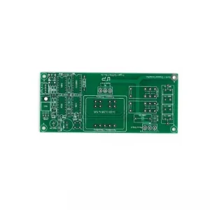
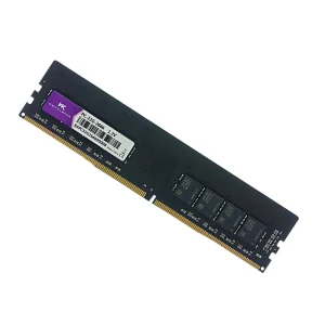
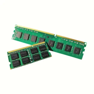
A: Our Automated Optical Inspection (AOI) catches microscopic defects that the human eye misses. In the context of high-speed DDR5 RAM or complex server motherboards, even a minute misalignment can lead to system instability. Our inspection ensures 100% signal integrity.