In modern enterprise architecture, memory capacity and high-fidelity bandwidth represent critical paths for system reliability, compute density, and application throughput. As AI inference engines, real-time edge processing hubs, and next-generation cloud architectures scale, the demand for high-performance memory modules grows. CoreByte Storage Technology Co., Ltd. addresses this demand by offering custom OEM expandable memory solutions engineered to survive under complex thermal and computational workloads.
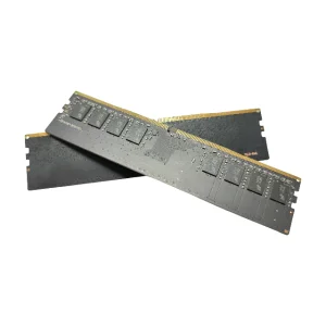
Transitioning from older standards to DDR5 involves managing changes in physical signaling, power distribution, and validation. With built-in Power Management Integrated Circuits (PMICs) and dual 32-bit independent subchannels, today's DRAM modules demand highly advanced PCB routing designs and reliable thermal management systems. CoreByte Storage Technology acts as a specialized R&D partner and manufacturer, helping system integrators configure and deploy tailored memory architectures that mitigate risks like signal attenuation, thermal throttling, and multi-component conflicts.
"For enterprise deployments, memory reliability is not just about raw data rates. It requires careful optimization of signal paths, robust thermal cooling interfaces, and complete compatibility across diverse chipset ecosystems."
Established in 2016, CoreByte Storage Technology Co., Ltd. is a dedicated manufacturer of high-performance DDR5/DDR4 memory modules and customized DRAM systems. The company specializes in supplying OEM systems, cloud infrastructure providers, and data centers. Headquartered in a modern facility with a core footprint of 320㎡ dedicated to advanced diagnostic testing, testing validation, and client services, CoreByte has built a strong trade presence globally.
With an annual export revenue of approximately USD 12 million, the team brings 6 years of focused export expertise and over 9 years of deep industry experience in semiconductor assemblies, memory module designs, and high-frequency PCBA configurations. Our operations are driven by a commitment to E-E-A-T (Experience, Expertise, Authoritativeness, and Trustworthiness) standards, ensuring that every product complies with international quality metrics.
Quality control is integrated into every phase of our manufacturing. CoreByte implements structured, ISO9001-based quality management systems alongside Automated Optical Inspection (AOI) and high-temperature aging chambers. These processes verify signal traces, solder joints, and raw component integrity under thermal stress. The quality control department employs 45 dedicated inspectors to manage high-yield reliability for production batches before they ship.
CoreByte supports clients in North America, Europe, Southeast Asia, and the Middle East. Supported by a network of over 1,200 supply chain partners, CoreByte maintains access to critical components, including DRAM die from major silicon foundries, high-Tg PCBs, and PMICs. This helps us ensure stable production and short lead times even when the market is volatile.
Southern China's electronics clusters, particularly in Shenzhen and Dongguan, provide a highly integrated hardware manufacturing ecosystem. For global companies sourcing custom memory solutions, this cluster offers several distinct advantages:
Proximity to key packaging, assembly, and testing facilities enables quick access to raw silicon, reducing component procurement times and speeding up overall production schedules.
Our design and manufacturing teams work closely together, allowing us to turn customer requirements into physical PCB prototypes within days. This accelerates validation and time-to-market.
We support both high-volume production runs and smaller, highly customized batches. Our facilities can easily scale to meet fluctuating demand without sacrificing quality.
CoreByte leverages this geographical advantage to source high-grade substrate materials, high-performance SMT lines, and specialized testing equipment. This proximity allows us to minimize freight overheads, shorten the supply chain, and manage export documentation efficiently for our global clients.
The enterprise memory landscape is undergoing structural changes driven by the need for more bandwidth per CPU core. Understanding these developments is essential for planning long-term hardware deployments:
CoreByte monitors these industry trends to update our product designs regularly. Our engineering team updates our product catalog each year, offering solutions that support new platforms from AMD, Intel, and ARM architectures.
Modern memory systems must perform reliably across a wide range of operational environments. CoreByte designs and manufactures memory modules for several key application scenarios:
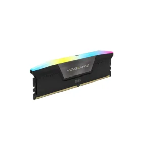
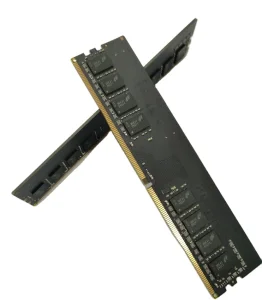
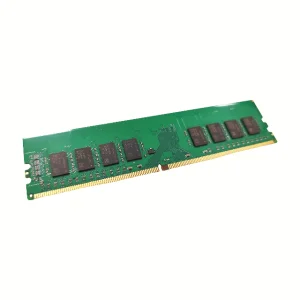
We supply cloud datacenters with high-density DDR5 RDIMMs featuring on-module PMICs and thermal sensors. These modules are built to handle high-bandwidth workloads, virtualization, and large-scale cloud databases with low failure rates.
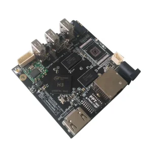
For harsh edge environments, we produce SO-DIMMs and custom PCBA boards designed to withstand vibration and wide temperature ranges. These are optimized for smart manufacturing, IoT gateways, and outdoor machinery control units.
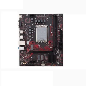
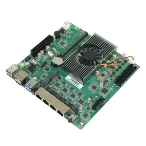
Our mini-ITX boards and low-profile memory options are used in firewalls, routers, and 5G base stations. These systems are configured for high uptime, low power draw, and consistent data throughput.
CoreByte also offers customization services for specialized industries, including medical imaging systems, transportation monitors, and custom consumer appliances. By working directly with our engineers, clients can specify layout constraints, BIOS settings, and testing criteria to fit their exact system designs.
Deploying customized memory modules requires careful design and testing. CoreByte utilizes a clear, step-by-step framework to transition designs from the concept phase to final production:
1. Architecture & Specification Definition: We work with your engineering team to define performance targets, interface types (DDR5, DDR4, custom pins), thermal profiles, and physical space limits.
2. PCB Layout & Signal Simulation: Our R&D engineers design multi-layer PCBs (up to 10 or 12 layers) using specialized tools to simulate signal integrity, manage impedance, and minimize crosstalk.
3. Prototype Sample Fabrication: We manufacture a test batch of prototype modules using SMT lines. These samples undergo initial functional testing and BIOS verification.
4. Verification & Stress Testing: Prototypes are run through thermal chambers, high-temperature burn-in ovens, and hardware testers like Advantest to evaluate long-term reliability.
5. Production & Quality Control: Once approved, we begin volume manufacturing. Every batch is verified using AOI systems and final functional tests before shipping.
This process reduces design risks, limits compatibility issues, and ensures compliance with CE, FCC, RoHS, and local regulatory standards.
To assist system integrators and procurement managers, our engineering team has compiled answers to frequently asked technical questions:
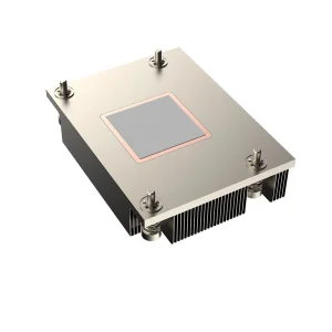
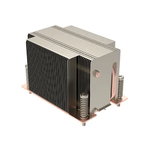
To maintain high manufacturing yields, our facilities utilize automated SMT placement, controlled reflow soldering, and specialized hardware testing suites. Below is a view into our manufacturing, packaging, and testing operations:
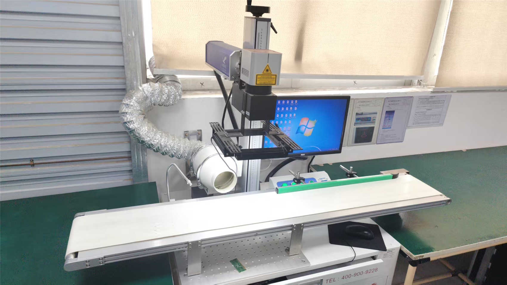
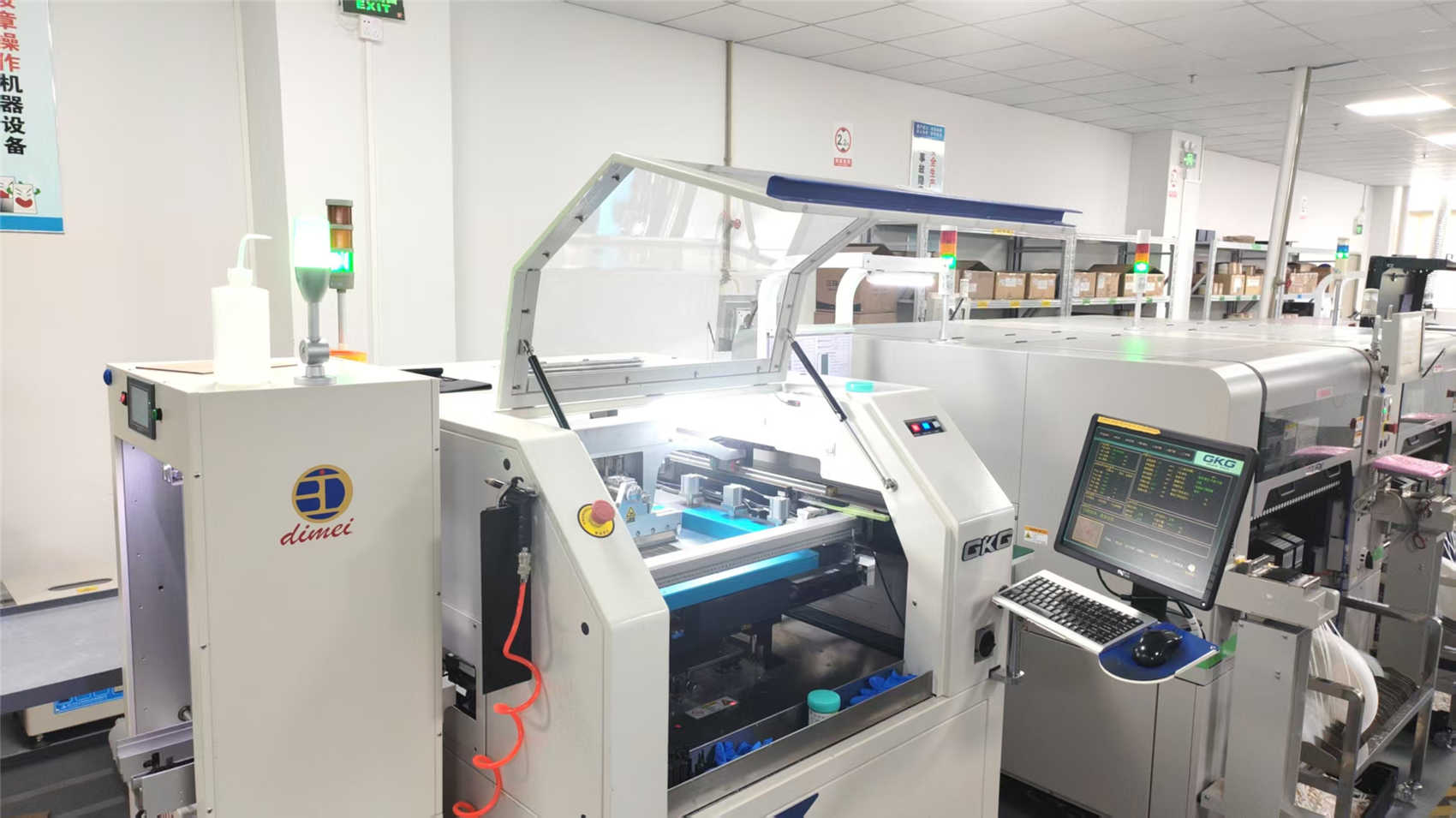

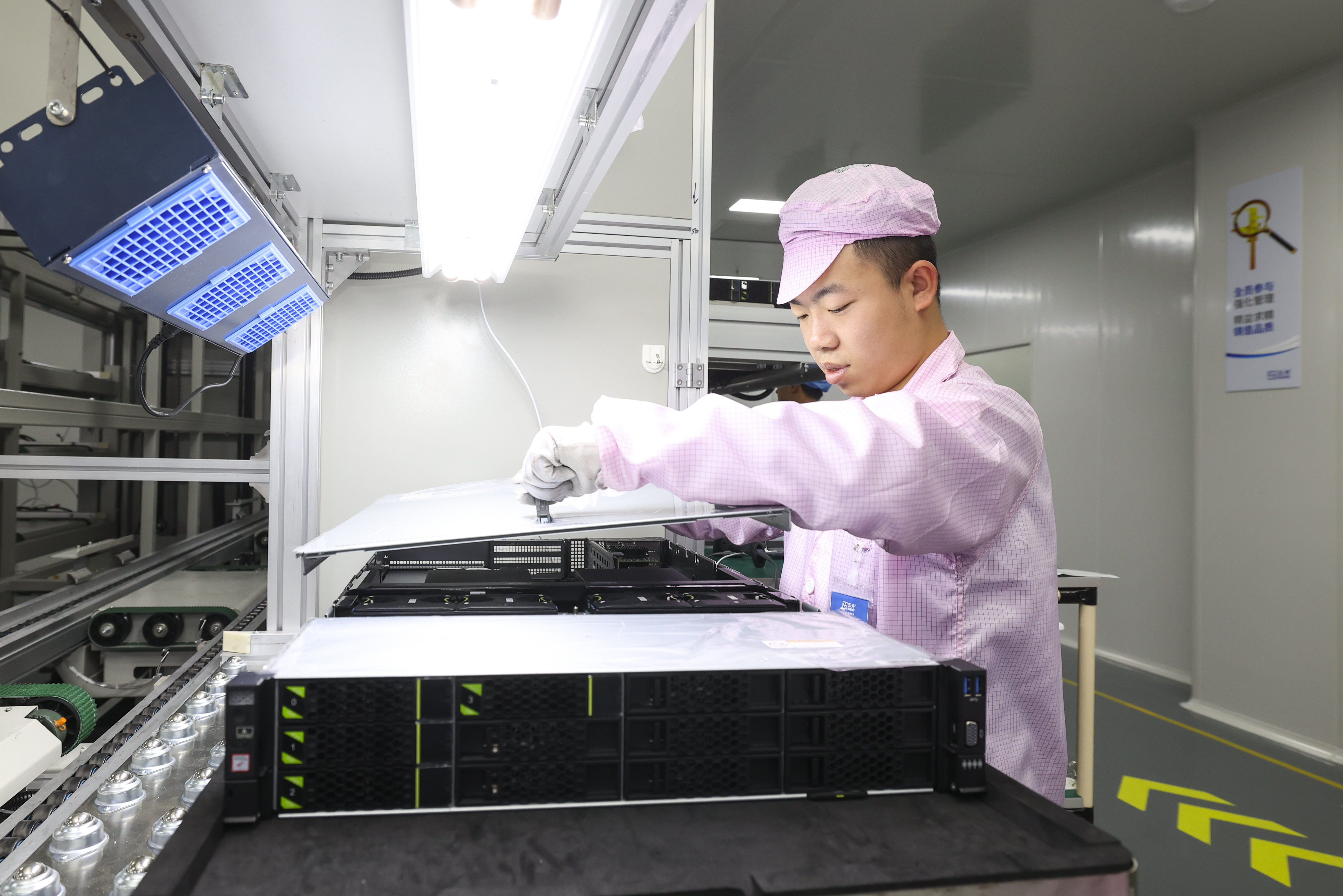
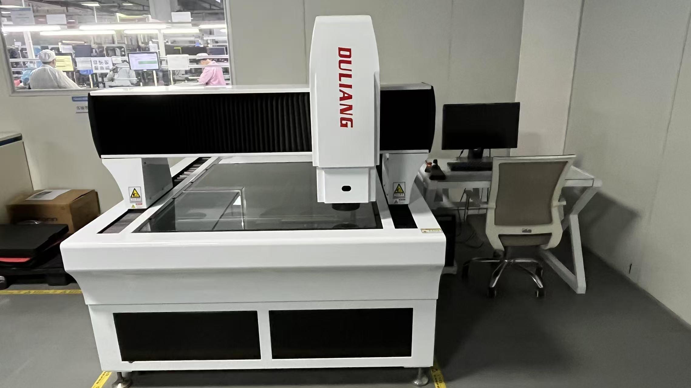
Our testing procedures are designed to meet ISO9001 standards, helping us deliver stable performance across all client deployments.