How RAM chips are made is becoming a critical question for buyers, designers, and data-center operators in 2026. RAM is no longer a simple commodity. Artificial intelligence workloads are increasing demand for high-bandwidth memory, advanced DRAM, and tighter power efficiency. TrendForce reported strong growth in HBM demand during 2024 and 2025, driven largely by AI accelerators. Gartner and IDC also identify memory availability as a significant factor in server procurement and technology planning.
The manufacturing journey begins with ultra-pure silicon wafers. Engineers print microscopic circuits using lithography, then implant dopants and deposit insulating layers. In a conventional DRAM cell, one transistor controls access to one capacitor. Robert H. Dennard, the DRAM inventor, described the core design as “one transistor and one capacitor.” That tiny capacitor stores electrical charge as data. It must be repeatedly refreshed because charge gradually leaks away. Small details matter. A speck of contamination can damage an entire wafer.
The best RAM chip suppliers combine process control, yield management, packaging expertise, and dependable delivery. Samsung Electronics, SK hynix, and Micron remain major global memory manufacturers, according to company filings and the Semiconductor Industry Association. Their advantage is not only factory scale. It also comes from years of refining etching, deposition, testing, and advanced packaging.
Still, supplier rankings deserve caution. Market leadership can change quickly when pricing, capacity, or technology shifts. A glossy specification sheet does not reveal every manufacturing weakness. This guide examines the leading 2026 suppliers and explains the physical steps behind modern RAM production. The process is impressive, but not perfect. That limitation matters.
RAM chips are semiconductor components that temporarily store data for active computing tasks. Unlike long-term storage, most RAM loses its contents when power disappears. This volatility sounds limiting, but it enables very fast access. A processor can retrieve working instructions, application data, and cached values without waiting for slower storage devices.
The main types include DRAM and SRAM. DRAM stores each bit in a capacitor and transistor, so it needs regular refreshing. It offers higher capacity and commonly supports system memory. SRAM uses multiple transistors to hold data without constant refresh. It is faster, but larger and more expensive per bit, making it suitable for processor cache. Modern categories also include synchronous DRAM, double-data-rate memory, low-power memory, and high-bandwidth memory. Their differences involve speed, power use, bandwidth, and physical design.
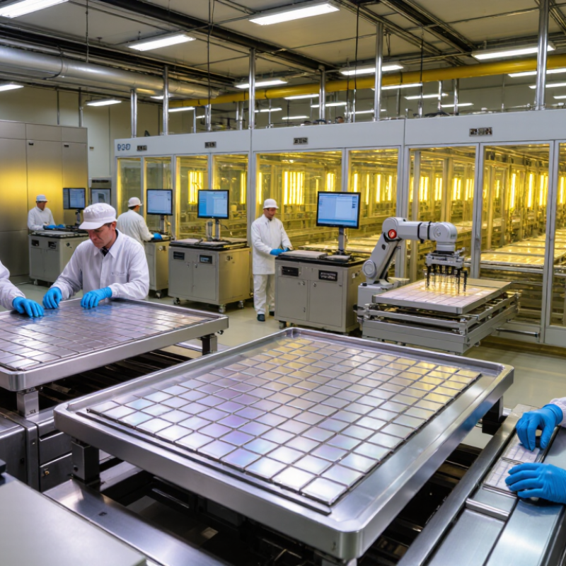
RAM chips begin with highly pure silicon wafers. Manufacturers deposit thin materials, apply patterned light-sensitive layers, and etch microscopic structures. Controlled doping changes how electricity moves through each region. Engineers then build memory cells, connect them with metal wiring, and test electrical behavior across many temperature conditions. Packaging protects the die and provides external connections. A tiny defect can affect an entire memory block. That remains a difficult manufacturing reality. In practical system design, capacity alone is not enough; timing, refresh behavior, heat, and workload patterns also influence real performance.
| RAM Category | Cell or Package Structure | Typical Interface or Organization | Typical Voltage Range | Main Performance Characteristic | Primary Applications | Core Function | Key Supplier Evaluation Criteria |
|---|---|---|---|---|---|---|---|
| SRAM | Usually a six-transistor bistable cell; does not require periodic refresh while powered. | Asynchronous or synchronous parallel interface; commonly organized by independent address and data buses. | Commonly about 1.0–3.3 V, depending on process generation and application. | Very low latency | Processor caches, network buffers, embedded systems, and high-speed control circuits. | Stores data temporarily with fast and predictable read/write access. | Access time, standby current, industrial temperature range, density, and long-term availability. |
| DRAM | Typically one transistor and one capacitor per memory cell; periodic refresh is required. | Row-and-column addressed array with multiplexed address signals and a data bus. | Commonly about 1.1–1.5 V for modern low-voltage generations. | High density | Computers, servers, embedded equipment, and general-purpose memory modules. | Provides dense, temporary working memory for processors and system controllers. | Density, data rate, timing compatibility, error support, thermal behavior, and qualification history. |
| DDR3 SDRAM | Double-data-rate synchronous DRAM with an 8n prefetch architecture. | Commonly 64-bit data width per unbuffered module, excluding optional error-correction bits. | Approximately 1.5 V; lower-voltage variants are available. | Mature and cost-effective | Legacy computers, industrial controllers, and equipment with established DDR3 designs. | Transfers data on both rising and falling edges of the clock. | End-of-life planning, compatible module organization, signal integrity, and supply continuity. |
| DDR4 SDRAM | Double-data-rate synchronous DRAM with an 8n prefetch architecture. | Commonly supports 64-bit module data paths, with additional bits possible for error correction. | Approximately 1.2 V for the standard memory interface. | Balanced capacity and bandwidth | Desktop systems, laptops, servers, workstations, and industrial computing platforms. | Offers higher density and bandwidth than earlier mainstream DDR generations. | Supported speed grades, module topology, error-correction options, validation data, and availability. |
| DDR5 SDRAM | Double-data-rate synchronous DRAM with an 8n prefetch architecture and split internal channels. | A standard module generally uses two independent 32-bit subchannels, totaling 64 data bits. | Approximately 1.1 V at the memory interface; modules commonly use onboard power-management circuitry. | High bandwidth and scalability | Current-generation PCs, servers, workstations, artificial-intelligence systems, and data centers. | Improves bandwidth, capacity scaling, and memory-channel efficiency for modern processors. | Supported data rates, module reliability, power-management design, error features, and platform validation. |
| LPDDR4 and LPDDR4X | Low-power synchronous DRAM designed for compact packages and reduced energy consumption. | Typically uses multiple narrow channels and a 16n prefetch architecture. | LPDDR4 is commonly around 1.1 V; LPDDR4X lowers the I/O voltage to approximately 0.6 V. | Low power per transferred bit | Mobile devices, tablets, thin notebooks, automotive electronics, and embedded products. | Reduces active and standby power while providing high bandwidth in space-constrained designs. | Power states, package size, thermal performance, retention behavior, and system-level validation. |
| LPDDR5 and LPDDR5X | Low-power synchronous DRAM with enhanced power-management and higher-speed signaling features. | Uses multiple channels and a 16n prefetch architecture; exact speed depends on the implementation. | Core and I/O voltages vary by implementation; low-voltage signaling is used to reduce energy consumption. | High mobile bandwidth | Premium mobile devices, edge computing, automotive systems, and energy-sensitive embedded platforms. | Delivers high memory throughput with dynamic frequency and power-control mechanisms. | Speed-grade qualification, thermal margins, package-on-package compatibility, power profiles, and availability. |
| GDDR6 | Graphics-oriented synchronous DRAM optimized for high-speed data transfers. | Uses independent channels and point-to-point connections with high-speed I/O signaling. | Typically about 1.35 V for the core memory supply, with implementation-dependent I/O requirements. | High graphics bandwidth | Graphics processors, gaming systems, professional visualization, and accelerator cards. | Moves large volumes of texture, frame-buffer, and compute data with high throughput. | Signal integrity, validated speed, thermal characteristics, package quality, and error behavior. |
| HBM2E and HBM3 | Multiple DRAM dies stacked vertically and connected with through-silicon vias and a silicon interposer. | Very wide interface; a common HBM stack uses a 1,024-bit interface per stack. | Low-voltage signaling; exact values depend on the HBM generation and system implementation. | Extreme bandwidth density | Artificial-intelligence accelerators, high-performance computing, networking, and advanced graphics. | Provides high bandwidth close to the processor while reducing the energy cost of long board-level traces. | Stack yield, thermal design, interposer compatibility, bandwidth qualification, and advanced packaging capability. |
| Manufacturing: Wafer Fabrication | Silicon wafers undergo oxidation, thin-film deposition, photolithography, etching, ion implantation, and metallization. | Repeated process layers form transistors, capacitors, word lines, bit lines, and peripheral circuits. | Process voltage depends on the memory generation and transistor technology. | Cell density and yield | All semiconductor RAM products. | Creates the memory-cell array and the circuits required for addressing, sensing, refresh, and data transfer. | Process control, defect density, design-rule capability, wafer yield, and electrical uniformity. |
| Manufacturing: Assembly and Packaging | Individual dies are separated, tested, assembled into packages, and connected using wire bonding, flip-chip, or advanced stacking methods. | Package type may include molded packages, multi-die packages, package-on-package, or stacked-die structures. | Package selection influences signal loss, heat dissipation, and allowable operating conditions. | Integration and reliability | Memory modules, mobile devices, graphics cards, servers, and embedded systems. | Protects the die and provides electrical, mechanical, and thermal connections to the host system. | Assembly yield, thermal resistance, package dimensions, mechanical reliability, and traceability. |
| Manufacturing: Testing and Qualification | Parametric tests, functional tests, speed-binning, burn-in, temperature testing, and reliability screening. | Testing verifies capacity, timing, voltage margins, refresh behavior, error features, and interface compatibility. | Products are tested across specified voltage and temperature limits. | Consistency and field reliability | Commercial, industrial, automotive, networking, and data-center applications. | Identifies defective or marginal devices before shipment and confirms compliance with specifications. | Test coverage, quality systems, failure-analysis capability, qualification standards, and lot traceability. |
A RAM chip temporarily stores data used by active computing tasks. It is volatile. Power loss usually erases its contents.
RAM holds instructions, application data, and cached values near the processor. This reduces waiting compared with slower storage devices.
DRAM uses capacitors and requires regular refreshing. SRAM uses multiple transistors and keeps data without constant refresh.
DRAM offers higher capacity and lower cost per bit. SRAM is faster, larger, and more expensive, so it suits processor cache.
Common categories include synchronous DRAM, double-data-rate memory, low-power memory, and high-bandwidth memory. They differ in speed, power, bandwidth, and design.
Production starts with highly pure silicon wafers. Engineers deposit materials, pattern light-sensitive layers, etch structures, and control electrical behavior through doping.
Automated probes check leakage, timing, voltage stability, and data retention. Functional testing also uses different frequencies, voltages, and temperatures.
Samples undergo long operation, thermal stress, and mechanical handling tests. X-ray inspection can reveal hidden connection faults. No screening method catches every future failure.
Review defect rates, delivery records, certifications, traceability, failure analysis, and regional logistics. Specifications alone can mislead. Documentation matters.
No. Timing, refresh behavior, heat, and workload patterns also affect performance. More capacity may still leave a system feeling slow.
This article explains RAM chips, their main types, and their essential role in temporarily storing data for fast access by computers, smartphones, and other electronic devices. It also reviews the qualities to consider when evaluating leading RAM chip suppliers in 2026, including production capacity, process technology, reliability, energy efficiency, and quality control. Without naming specific companies, the discussion focuses on how suppliers support the global demand for stable and high-performance memory products.
The section on How RAM chips are made follows the process from raw materials and silicon wafer preparation to circuit formation, layering, patterning, etching, doping, and electrical interconnection. After fabrication, each chip undergoes testing to identify performance or manufacturing defects. The chips are then separated, packaged, inspected, and tested again under different operating conditions. Together, these steps help ensure consistent speed, durability, compatibility, and reliable operation in a wide range of modern electronic devices.

 CoreByte